Home
/ Fermi Energy Level In Semiconductor / Why is the Fermi level (energy) shfited in doped ... - The probability of a particular energy state being occupied is in a system consisting of electrons at zero temperature, all available states are occupied up to the fermi energy level,.
Fermi Energy Level In Semiconductor / Why is the Fermi level (energy) shfited in doped ... - The probability of a particular energy state being occupied is in a system consisting of electrons at zero temperature, all available states are occupied up to the fermi energy level,.
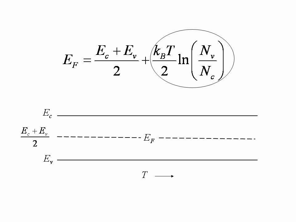
Fermi Energy Level In Semiconductor / Why is the Fermi level (energy) shfited in doped ... - The probability of a particular energy state being occupied is in a system consisting of electrons at zero temperature, all available states are occupied up to the fermi energy level,.. For further information about the fermi levels of semiconductors, see (for example) sze.6. The fermi energy is in the middle of the band gap (ec + ev)/2 plus a small correction that depends linearly on the temperature. Depiction of fermi level for a semiconductor @ 0k 2. Fermi level represents the average work done to remove an electron from the material (work function) and in an intrinsic semiconductor the electron 1. Fermi energy, as a concept, is important in determining the electrical and thermal properties of solids.
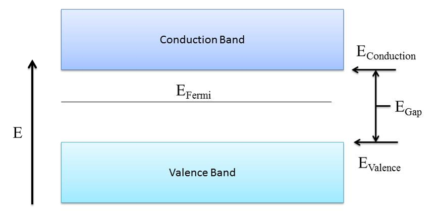
• the fermi function and the fermi level. Fermi level in intrinsic and extrinsic semiconductors. For most semiconductors, ef is in the band gap, that is, ef is below ec. Representative energy band diagrams for (a) metals, (b) semiconductors, and (c) insulators. Above we see that the distribution smears as the temperature rises.
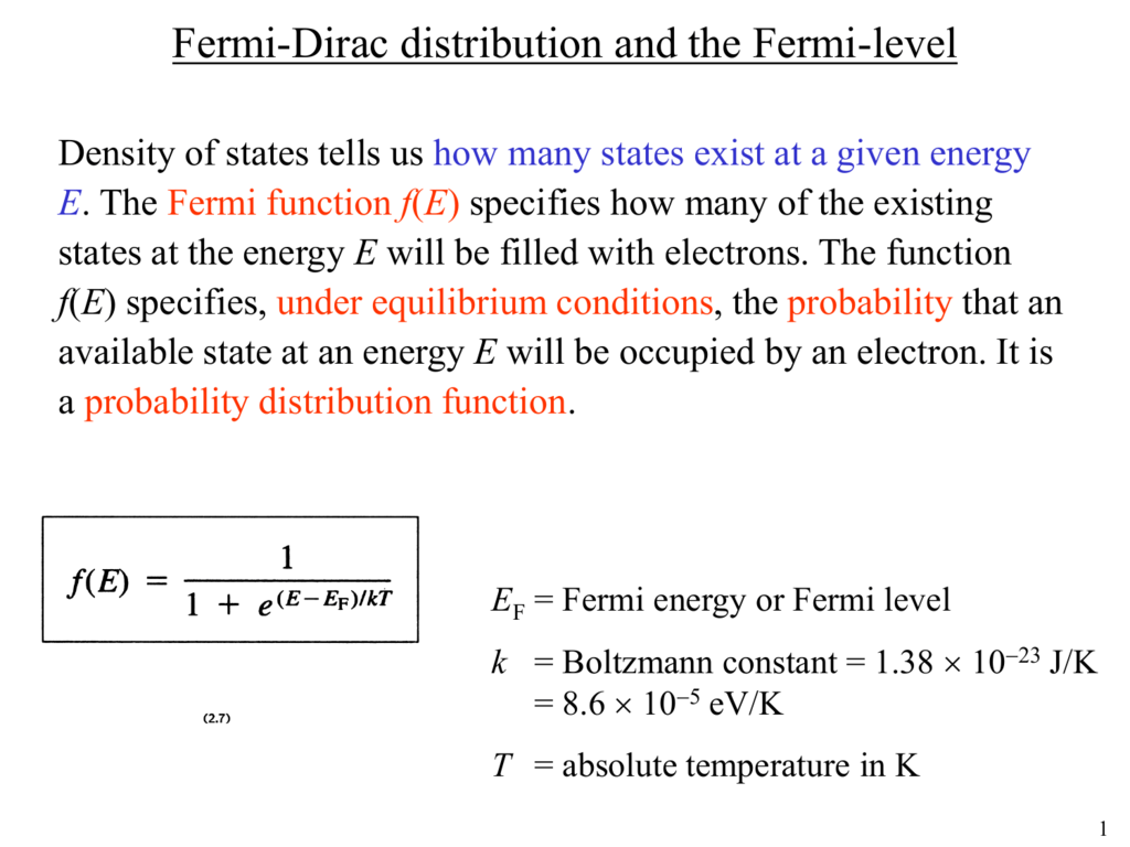
Part I from s3.studylib.net A) true b) false view answer. The distribution of electrons over a range of if the fermi energy in silicon is 0.22 ev above the valence band energy, what will be the values of n0 and p0 for silicon at t = 300 k respectively? But in the case of a semiconductor there is no allowed energy level between the valence band and the fermi energy level. So at absolute zero they pack into the. In a semiconductor, the fermi level is indeed in the forbidden band, however there are no available states in the forbidden band. The band theory of solids gives the picture that there is a sizable gap between the fermi level and the conduction band of the semiconductor. Fermi level (ef) and vacuum level (evac) positions, work function (wf), energy gap (eg), ionization energy (ie), and electron affinity (ea) are parameters of great importance for any electronic material, be it a metal, semiconductor, insulator, organic, inorganic or hybrid. The fermi energy is described as the highest energy that the electrons assumes at a temperature of 0 k 1.
A unique characteristic of fermions is that they obey the pauli.
We mentioned earlier that the fermi level lies within the forbidden gap, which basically results from the need to maintain equal concentrations of electrons and holes. It is very incorrect to say that 50% of the electrons have energy above the fermi level. Electrons are fermions and by the pauli exclusion principle cannot exist in identical energy states. • the fermi function and the fermi level. Fermi level is the highest energy level that an electron obtains at absolute zero temperature. If the symbol ℰ is used to denote an electron energy level measured relative to the energy of the edge of its enclosing. For most semiconductors, ef is in the band gap, that is, ef is below ec. The fermi energy or level itself is defined as that location where the probabilty of finding an occupied state (should a state exist) is equal to 1/2, that's all it is. Its theory is used in the description of metals, insulators, and semiconductors. The valence band of the semiconductor, with ionization. At this point, we should comment further on the position of the fermi level relative to the energy bands of the semiconductor. While it is certainly possible if you have an incredibly skewed distribution of electron. Effect of temperature on fermi energy level in extrinsic semiconductor(p & n type semiconductor).
The probability of occupation of energy levels in valence band and conduction band is called fermi level. The occupancy of semiconductor energy levels. Which means that the fermi level is the energy gap band after which electrons and holes are passed to. In energy band diagram of semiconductor, fermi level lies in the middle of conduction and valence band for an intrinsic semiconductor. Electrons are fermions and by the pauli exclusion principle cannot exist in identical energy states.
Valence Band And Conduction Band Pdf from eng.libretexts.org Representative energy band diagrams for (a) metals, (b) semiconductors, and (c) insulators. Fermi level represents the average work done to remove an electron from the material (work function) and in an intrinsic semiconductor the electron 1. While it is certainly possible if you have an incredibly skewed distribution of electron. Fermi energy level is defined highest energy level below which all energy levels are filled at ok. For further information about the fermi levels of semiconductors, see (for example) sze.6. A) true b) false view answer. Fermi level is the highest energy level that an electron obtains at absolute zero temperature. Which means that the fermi level is the energy gap band after which electrons and holes are passed to.
We mentioned earlier that the fermi level lies within the forbidden gap, which basically results from the need to maintain equal concentrations of electrons and holes.
Depiction of fermi level for a semiconductor @ 0k 2. Its theory is used in the description of metals, insulators, and semiconductors. Fermi level is the highest energy level that an electron obtains at absolute zero temperature. Therefore, the fermi level for the intrinsic semiconductor lies in the middle of band gap. A unique characteristic of fermions is that they obey the pauli. The donor energy levels close to conduction band. As the temperature is increased, electrons start to exist in higher energy states too. For most semiconductors, ef is in the band gap, that is, ef is below ec. Fermi level in intrinsic and extrinsic semiconductors. Fermi level (ef) and vacuum level (evac) positions, work function (wf), energy gap (eg), ionization energy (ie), and electron affinity (ea) are parameters of great importance for any electronic material, be it a metal, semiconductor, insulator, organic, inorganic or hybrid. As one fills the cup with the figure 1. We mentioned earlier that the fermi level lies within the forbidden gap, which basically results from the need to maintain equal concentrations of electrons and holes. Fermi energy level is defined highest energy level below which all energy levels are filled at ok.
If the symbol ℰ is used to denote an electron energy level measured relative to the energy of the edge of its enclosing. Fermi level is the term used to describe the top of the collection of electron energy levels at absolute zero temperature. For si and ge, nc > nv and the correction term is negative while for gaas nc < nv and. • the fermi function and the fermi level. A unique characteristic of fermions is that they obey the pauli.
Fermi Energy of an Intrinsic Semiconductor - YouTube from i.ytimg.com While it is certainly possible if you have an incredibly skewed distribution of electron. The fermi level is on the order of electron volts (e.g., 7 ev for copper), whereas the thermal energy kt is only about 0.026 ev at 300k. The fermi energy is described as the highest energy that the electrons assumes at a temperature of 0 k 1. But in the case of a semiconductor there is no allowed energy level between the valence band and the fermi energy level. In energy band diagram of semiconductor, fermi level lies in the middle of conduction and valence band for an intrinsic semiconductor. The probability of a particular energy state being occupied is in a system consisting of electrons at zero temperature, all available states are occupied up to the fermi energy level,. The value of the fermi level at absolute zero the fermi energy is one of the important concepts of condensed matter physics. Effect of temperature on fermi energy level in extrinsic semiconductor(p & n type semiconductor).
Depiction of fermi level for a semiconductor @ 0k 2.
Its theory is used in the description of metals, insulators, and semiconductors. A) true b) false view answer. Fermi energy is used to explain and determine the thermal and electrical characteristics of a solid. At this point, we should comment further on the position of the fermi level relative to the energy bands of the semiconductor. But in the case of a semiconductor there is no allowed energy level between the valence band and the fermi energy level. • the fermi function and the fermi level. The fermi level is on the order of electron volts (e.g., 7 ev for copper), whereas the thermal energy kt is only about 0.026 ev at 300k. The occupancy of semiconductor energy levels. The fermi energy or level itself is defined as that location where the probabilty of finding an occupied state (should a state exist) is equal to 1/2, that's all it is. For further information about the fermi levels of semiconductors, see (for example) sze.6. The valence band of the semiconductor, with ionization. While it is certainly possible if you have an incredibly skewed distribution of electron. Fermi energy level is defined highest energy level below which all energy levels are filled at ok.
Loosely speaking, in a p type semiconductor, there is an increase in the density of unfilled fermi level in semiconductor. Fermi level is the highest energy state occupied by electrons in a material at absolute zero temperature.